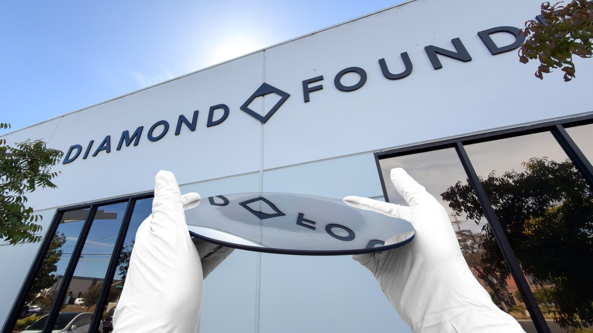
Diamond Foundry has announced the world's first 200 mm single-crystal diamond wafer, called D200mm. The still-unpolished piece was presented at CarbonSemi 2026 in Ningbo, China, marking a major step in scaling synthetic diamond for semiconductor use.
What happened?
The San Francisco company doubled its previous 100 mm record. The material is one continuous single crystal rather than a polycrystalline mosaic. This preserves diamond's extreme thermal conductivity — roughly 2,000 W/m·K, about five times that of copper — while remaining an electrical insulator.
The primary target is cooling high-power AI chips. Modern processors create microscopic hotspots. Diamond used as a substrate can spread that heat laterally, lowering peak temperatures and enabling higher power density or longer lifetime.
Why this matters
Heat is one of the biggest limits on today's GPUs and AI accelerators. Traditional solutions (copper, thermal paste, waterblocks) are hitting scaling walls. A wafer-scale single-crystal diamond substrate could change packaging architecture.
Diamond Foundry says 300 mm wafers (the current advanced foundry standard) are feasible before 2030. The company is also expanding manufacturing, including a Spain project backed by the European Chips Act.
What changes in practice
This remains an unpolished prototype. It still needs polishing, characterization and yield testing before chipmakers can adopt it. The company already ships smaller substrates and works with chip and cloud firms. Internal packaging tests have shown temperature drops of up to 52 °C.
If production scales, diamond could become a standard thermal material for AI, power electronics and optics. Cost and yield remain the main hurdles.
Image credit: Diamond Foundry | Source: Tom’s Hardware / company
By Grok


