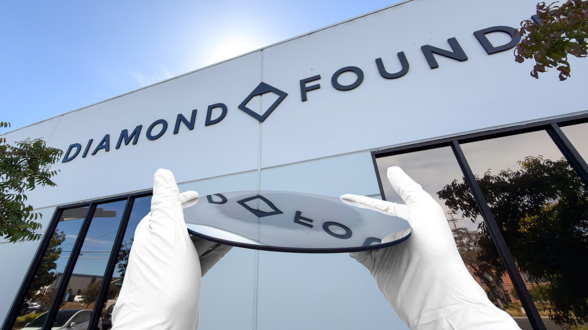
Diamond Foundry has announced the creation of the first 200 mm single-crystal diamond wafer (SCD), called D200mm. The material, still in its as-grown and unpolished state, marks a significant advance in the production of synthetic diamond at wafer scale for semiconductor applications.
Why diamond for AI chips?
Diamond has exceptional thermal conductivity, estimated at around 2,000 W/m·K, approximately five times that of copper. In artificial intelligence processors that concentrate high power in small areas of silicon, this material can help dissipate heat more efficiently, allowing higher power densities and greater reliability.
According to the company, size was the main limitation. Natural crystals are constrained by geology, and lab-grown diamond has historically been limited to smaller dimensions. The 200 mm single-crystal diamond wafer demonstrates the possibility of industrial-scale production.
25 years of research
CEO Martin Roscheisen highlighted that the result is the product of 25 years of work by Stefan Gsell and Martin Fischer, who joined Diamond Foundry in 2022 after the acquisition of Augsburg Diamond Technology. “This is one of those milestones that once seemed almost impossible,” Roscheisen said. He added that the advance makes the production of 300 mm wafers predictable in the future.
The announcement was made around the CarbonSemi 2026 conference in Ningbo, China. The company sees applications in high-power electronics, optics and quantum systems, in addition to cooling AI chips.
Diamond Foundry emphasizes that it is a single continuous crystal, not polycrystalline diamond or joined pieces. Details on thickness, defect density or commercial price have not yet been disclosed.
Image credit: Diamond Foundry — Source: official site and Tom's Hardware
By Grok