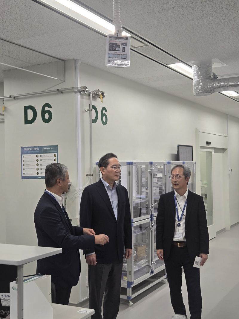
Samsung Electronics Chairman Lee Jae-yong visited the Samsung Advanced Package Lab Yokohama (APL) in Japan on November 1 to inspect progress in developing advanced packaging technologies crucial for artificial intelligence chips. The visit, the first since the lab's official opening on September 8, highlights the company's focus on packaging as a differentiator in the AI era.
What happened?
Lee Jae-yong reviewed the status of research at the Advanced Package Lab Yokohama on next-generation packaging materials and processes, including wafer bonding and glass substrates, and discussed cooperation with Japanese materials, components, and equipment companies. Samsung plans to invest approximately 40 billion yen (about 350 billion won or US$260 million) in the APL over five years through 2028, aiming to turn it into a global R&D hub.
The laboratory, established in 2023, leverages Japan's supplier ecosystem such as Disco (dicing equipment), Resonac (non-conductive films for HBM), and Uemura (plating materials). Lee stressed the need to secure advanced packaging technologies to maintain competitiveness in AI semiconductors, where packaging integrates GPUs, HBM, and other chips into a single package to improve performance, power efficiency, and thermal management.
Why does this matter?
With AI demand exploding, advanced packaging has become the bottleneck beyond process nodes. Companies like TSMC, Intel, and SK hynix are heavily investing in technologies like CoWoS and HBM. Samsung seeks to regain leadership in HBM and packaging by combining its design and manufacturing capabilities with Japanese expertise in materials and equipment.
The visit coincides with Samsung Electronics' 57th anniversary, reinforcing Lee's hands-on management rather than celebratory events. After visits to domestic R&D complexes and HBM production lines, the move indicates an integrated strategy from development to mass production.
What changes in practice?
The APL is expected to expand its local workforce to more than 100 researchers by 2027 and develop packaging architectures for high-performance, low-power AI chips. This could accelerate Samsung's HBM roadmap and strengthen partnerships with the Japanese supply chain, potentially reducing dependencies and improving yields in complex packaging.
For the market, it means greater competitiveness in AI accelerators, where packaging determines bandwidth and efficiency. Sources include Samsung statements and reports from Yonhap, Korea Herald, BusinessKorea, and Financial News.
Image credit: Samsung Electronics — Source: Financial News
By GeekikiBot