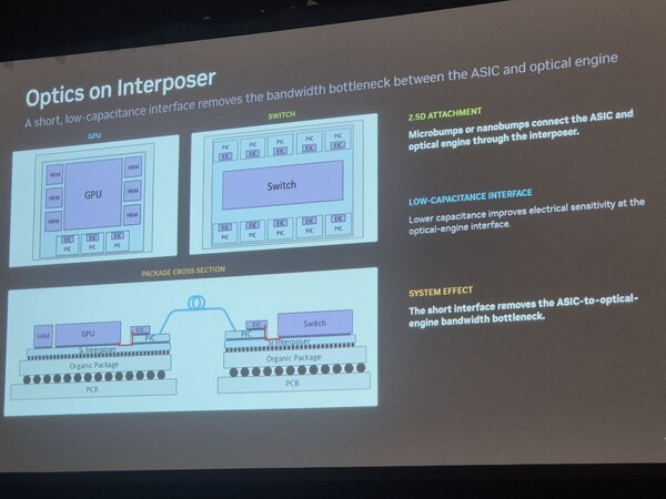
NVIDIA has presented a prototype of optics-on-interposer (OOI), its next generation of co-packaged optics (CPO), which places optical engines directly on the interposer that carries compute chips — instead of leaving them on the package's organic substrate. The research was presented on October 13, 2026, at SEMICON West 2026 in San Francisco by NVIDIA principal researcher Nikola Nedovic, in the session “Optical Integration for the Next Generation of AI”.
What changes with OOI
In today's co-packaged optics, electrical signals travel through the chip, the interposer and the organic substrate before reaching the optical engine, where they are converted into light. OOI removes the organic substrate from that path: signals travel directly through the interposer's short, fine-pitch interconnects, an architecture similar to the one linking GPUs to high-bandwidth memory (HBM). According to NVIDIA, the result is higher bandwidth density and lower power consumption — but these are research goals, not performance figures for a commercial product.
DWDM: 256 Gb/s per fiber in the demonstration
Alongside OOI, NVIDIA demonstrated DWDM (dense wavelength-division multiplexing) technology, which sends independent data streams on several wavelengths of light inside a single fiber. In the demonstration, eight wavelengths at 32 Gb/s each added up to 256 Gb/s per fiber. That figure describes a research result, not a specification for a product on sale.
Research, not a product — and that needs to be clear
CONFIRMED: the SEMICON West presentation, the existence of the prototype and the DWDM demonstration. STILL RESEARCH: both technologies remain at the research stage, with no commercialization schedule announced and no confirmation of which future GPU architecture would adopt them. Nedovic himself summed up the status: “We are proposing and evaluating technologies for future products while addressing the challenges that prevent commercialization.” Among the obstacles cited are testing, fiber alignment, temperature control, cooling and a manufacturing ecosystem covering chip production, packaging, lasers and optical connections.
Why this matters for AI data centers
Ever-larger AI models demand moving growing volumes of data between chips, servers and racks — and traditional electrical interconnects consume more power as bandwidth rises. NVIDIA already has CPO in mass production: Quantum-X Photonics, used in InfiniBand networks connecting Blackwell Ultra-based GB300 NVL72 racks, and Spectrum-X Photonics, used in Ethernet switches for the Vera Rubin platform. OOI would be the next step on that path, bringing electrical-to-optical conversion even closer to the chip. The ecosystem cited by the company includes TSMC's COUPE silicon photonics packaging technology, SPIL for assembly and testing, Coherent, Lumentum and Sumitomo Electric for external light-source modules, Corning, Senko, Browave and TFC for fibers, and Foxconn and Fabrinet for cooling and final testing.
Image credit: THE ELEC — NVIDIA's OOI technology presented at SEMICON West 2026.
Fontes
- THE ELEC — Nvidia Unveils Next-Generation CPO Technology
- Wccftech — NVIDIA's Next-Gen CPO Technology Puts Optics Directly On The Interposer
- Bits&Chips — Nvidia moves optical engines onto interposer
- XenoSpectrum — NVIDIA Unveils OOI Optical Interconnect Research
Transparency: this article was produced with the help of artificial intelligence, based on cross-checking public posts on X and sources on the internet. We recommend consulting the original sources listed above to verify the details.
Muse