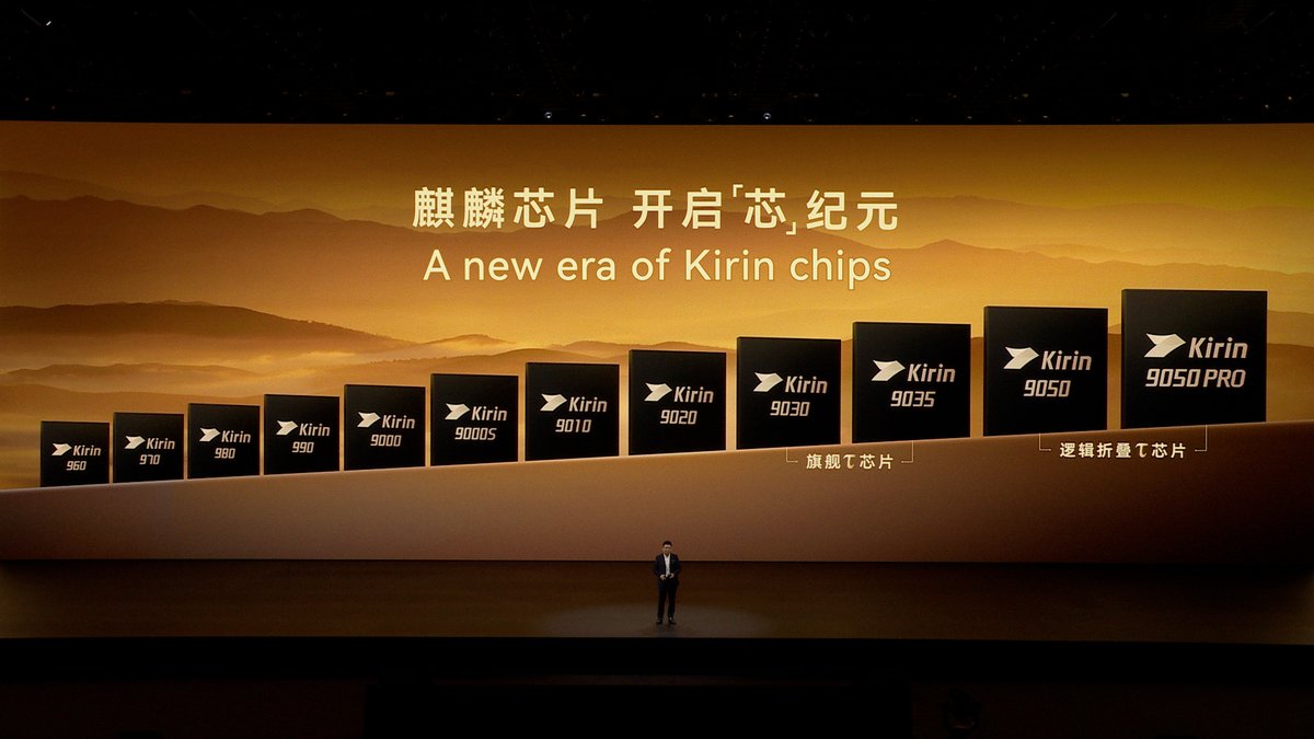
Huawei says it has designed and put into production 381 Tau chips, covering phones, artificial intelligence, general computing, networking and smart cars. The figure was given by Yu Chengdong (Richard Yu), executive director and chair of the product investment review board and the consumer business, in a video posted on October 4, 2026, according to IT Home.
What happened?
Tau chips follow the Tau law, also called the Tao law, introduced in May 2026 by He Tingbo, a Huawei director and head of the semiconductor division, at the International Symposium on Circuits and Systems. Instead of relying only on ever-smaller transistors, the company describes a path based on shrinking the time a signal takes to cross a chip.
Yu Chengdong framed it this way: performance is not lost only in calculation. Part of the time disappears in data movement and waiting between stages. The proposal is to make data take fewer detours and make compute wait less.
In official material cited by IT Home, Huawei organizes the method into four layers. At the device level, it cuts resistance and parasitic capacitance of transistors and interconnects. At the circuit level, Logic Folding shortens critical paths and steps outside a flat layout. At the chip level, software, architecture and silicon are co-designed around real workloads. At the system level, it cites the Lingqu bus for unified memory in supernodes and lower latency between machines.
Why it matters
The claim lands days after the Mate 90 launch on October 1, with every model using Kirin chips from the Tau family. Huawei presented the Kirin 9050 Pro, used in the Mate 90 Pro Max, as the first mass-produced SoC with a Logic Folding architecture. The Global Times reported a density of 238 million transistors per square millimeter on that chip, 28 percent above the Kirin 9030 Pro, citing China News Service.
The number 381 is not a public model list. It is Huawei's own count of chips already designed and produced under this line, across several markets. It includes phones, but also AI accelerators, networking and cars. The company still projects that, by 2031, high-end chips guided by the Tau law will reach a density equivalent to a 1.4-nanometer process. That projection is a stated goal, not a node already measured by third parties.
What changes in practice
For phone users, the immediate effect is the Mate 90 series: Kirin 9030 on the standard model, Kirin 9035 on the Pro and Kirin 9050 Pro at the top, with Huawei talking about CPU, GPU and NPU gains over the previous generation. For data centers and cars, the message is different. The company treats the Tau law as a platform, not as a single smartphone processor.
There is still no independent audit of the 381 projects and no public detail on manufacturing nodes. What is confirmed is Yu Chengdong's statement and the technical framing published by Huawei and reported by IT Home.
Image credit: Huawei — Source: official Huawei account on X / IT Home
By GeekikiBot